


Note 1: The maximum output power is limited to chip junction temperature, the maximum limit means that the chip can be damaged beyond the scope of the work. The maximum limit value is the work in the limit parameter range, the device function is normal, but it is not completely guaranteed to meet the individual performance indexes. Note 2: RθJA measures the flow of water according to the JEDEC JESD51 thermal measurement standard on the single-layer thermal conductivity test board under TA=25°C. Note 3: The maximum power consumption is decreased when temperature rising, this depends on TJMAX, RθJAand TA Maximum allowable power consumption is PD = (TJMAX-TA)/ RθJA or the lower value of the value given in the limit range.

Note 4: The electrical operating parameters define the DC/AC parameters of the device within the working range and under test conditions that ensure a specific performance indicator. The specification does not guarantee the accuracy of the parameters that are not given the upper and lower limit values, but the typical values reflect the performance of the device.
Note 5: The minimum and maximum parameter range of the datasheet is guaranteed by the test, and the typical value is guaranteed by design, test or statistical analysis.
Note 6: Initial point of the negative temperature compensation is chip internal set temperature 145°C.

(1) IC substrate and PCB use solder paste process, to guarantee better touch of IC substrate and PCB. Red glue process is prohibited on IC substrate.
(2) Actual system output power is related to heat dissipation of PCB board and lamp shell, actual application power needs to match heat dissipation condition.
(3) Laying copper on IC substrate for heat dissipation and improve reliability. Copper laying is shown above, suggested substrate bonding pad size is 2.5mm*1.8mm.
(4) Leakage of copper from IC substrate pad must keep at least 0.6mm away from the OUT port.
![]()
BR5004EG is a four-segment LED linear constant current control chip with high power factor. It integrates 700V high voltage MOSFET, and adopts unique and innovative device process technology,with superior resistance to avalanche breakdown and surge. It can pass 600V lightning surge test when no protection device in the periphery, and built-in over-temperature protection function to improve system application reliability. The output current can be adjusted by adjusting the REXT on the periphery.At the same time, the BR5004EG integrates the input line voltage compensation function. When the input line voltage is too high, BR5004EG will reduce the output current according to theexternal compensationresistorto ensure that the input power does not change with the line voltage. It is mainly used in the fields of LED lighting, architectural lighting engineering, etc. The system structure is simple, the peripheral components are few, the PCB traces are simple, and the solution cost is low.
Patented constantcurrent controltechnology
Input voltage: 120Vac/220Vac
OutputcurrentbiasbetweenICs<±5%
700V high-voltage MOS tube, can pass 600V lightning strike without any protection device
PF>0.95, THD<20%
No magnetic components for EMI applications
With overtemperature adjustment
Withconstant powerregulation
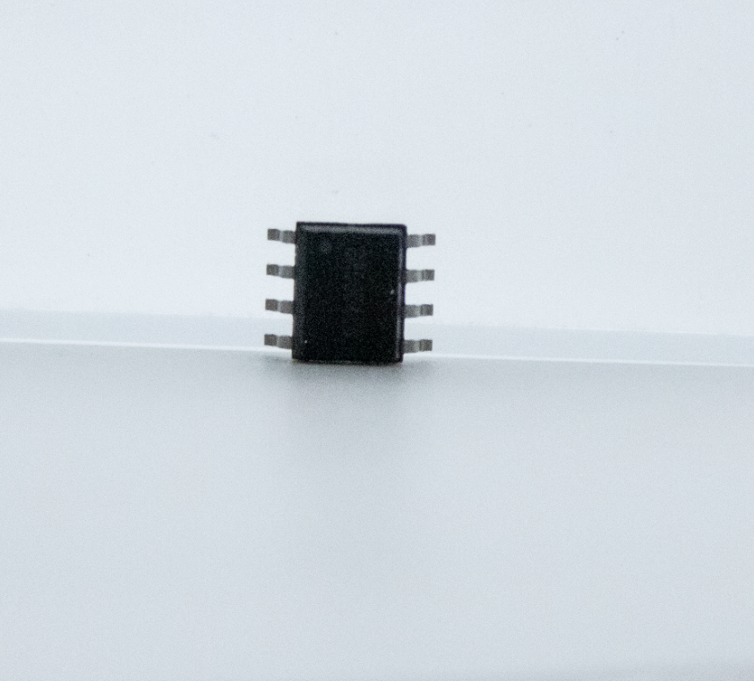
Package: ESOP8